A new version of this project is available here
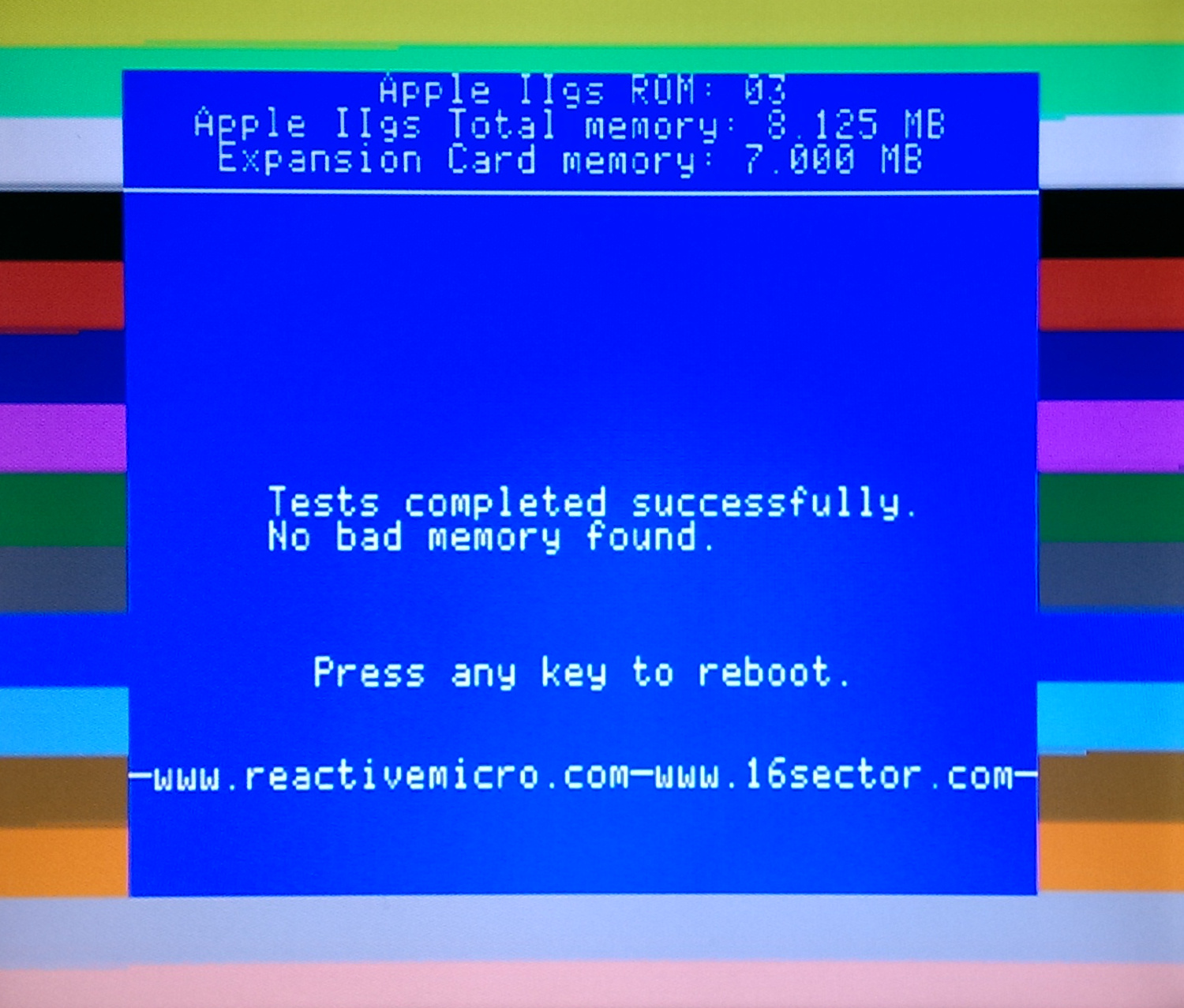
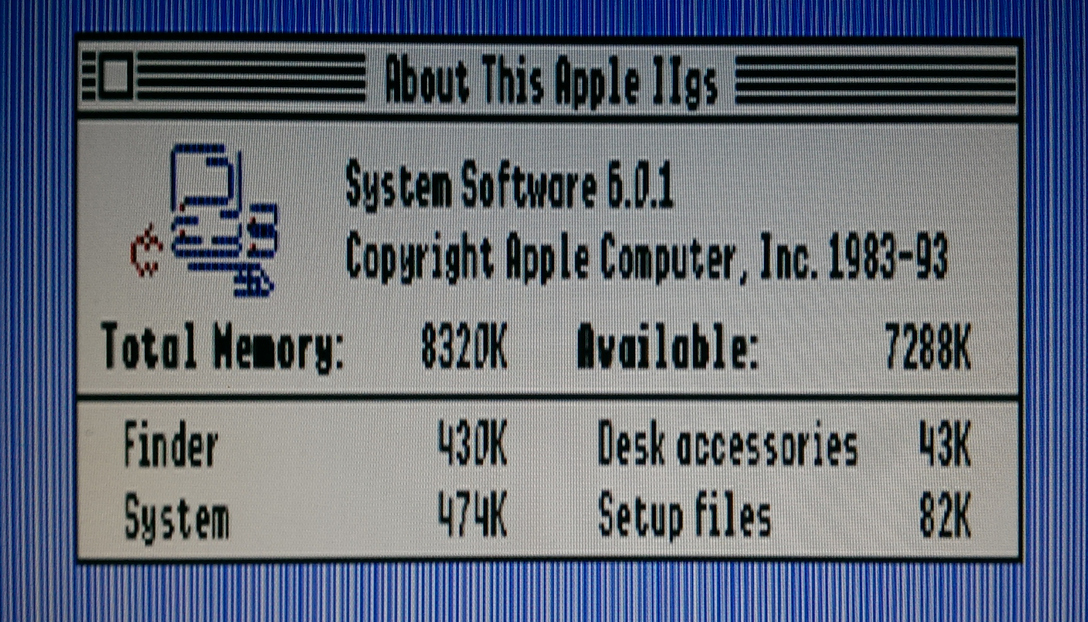
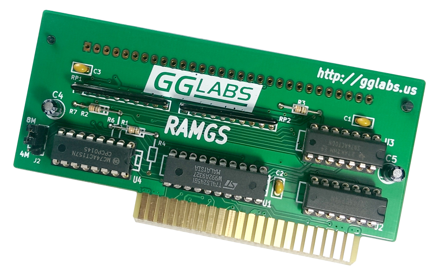 The apple IIgs is the most advanced computer in the Apple II series. Equipped with a 65c816 8/16-bit CPU with 24-bit address space it could address up to 16MB of memory. The original rom 01 model shipped with 256KB of fast RAM, the revised rom 3 shipped with 1MB (both had an additional 128KB of standard RAM and 64KB of sound RAM). RAMGS is a newly designed 8MB expansion card for this great classic computer.
This design builds on what we learned building the older RAMGS-MAX-A00 and the first generation RAMGS. Based on user feedback we replaced the 16 ZIP memories with just one 30-pin SIMM. This allowed us to reduce the PCB size for the 8MB configuration to 100x50mm.
U1 is a bi-directional buffer for the data bus. A low on the CSEL signal is required to read the DRAM data. The address bus FRA0-FRA9 is connected though series termination directly to the corresponding SIMM pins (note the signal swaps to simplify the routing). The circuit formed by U2A and U3 is necessary to add support for 4Mbit and 16Mbit DRAMs (see section at the end of the article for a detailed explanation).
U4 multiplexes CROW0, CROW1 and CROW2 to generate A10 (U4A) and A11 (U4B) for the SIMM. The connection of CROW0 to both U4A and U4B is to enable 4K refresh SIMMs. The extra two multiplexers U4C and U4D are used to generate a small delay necessary to ensure the hold time at the SIMM input is within specification.
The card can be configured for 1, 4 or 8MB (the 8MB configuration requires a 16MB SIMM half of which is unused).
The jumper J2 can be used to reduce the memory to 4MB in case of incompatibilities.
| SIMM | J2 | Available Memory |
|---|---|---|
| 1MB | N/A | 1MB |
| 4MB | N/A | 4MB |
| 16MB | 2-3 | 4MB |
| 16MB | 1-2 | 8MB |
The card accepts most 30-pin SIMMs from 1MB to 16MB (both parity and non-parity). All common configurations (2,3,8 and 9 chips) are fully supported. 4MB SIMMs using 2K and 4K refresh chips are supported. 256KB SIMMs should work but have not been tested.
Address Drive Strength
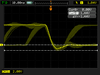
Most vintage expansion cards buffer the address to the drams on the card. After extensive probing on our previous cards it turns out that the buffers are unnecessary on the ramgs because of the limited loading (2-9 loads depending on the SIMM type and size) and short traces (about 80mm). For comparisons the apple 1MB expansion card has 32 loads and traces exceeding 300mm. Actually the FPI I/O drive is already too strong for the ramgs layout given the negative overshoot exceeds 2V in the scope captures.
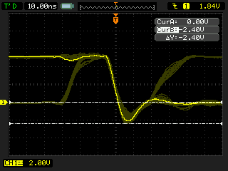
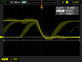
Adding series termination on the address lines reduces the overshoot at the expense of slower rise and fall time. The following two images show the effect of 56ohm and 100ohm series termination.
4Mbit Support
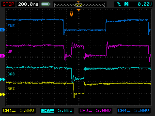
The Apple IIgs seems to perform only standard read cycles, early write cycles and CAS before RAS refresh cycles. We have not seen any fast page mode nor read-modify-write cycles.
Upon close inspection of the memory datasheets is clear that the CAS before RAS refresh cycle is different between the 1Mbit and the 4Mbit parts. In particular, the 4Mbit devices require WE to be high at the falling edge of RAS (WE is a don't care in the 1Mbit devices). Issuing a RAS before CAS refresh cycle with WE low on the 4Mbit DRAM enables the device test mode.

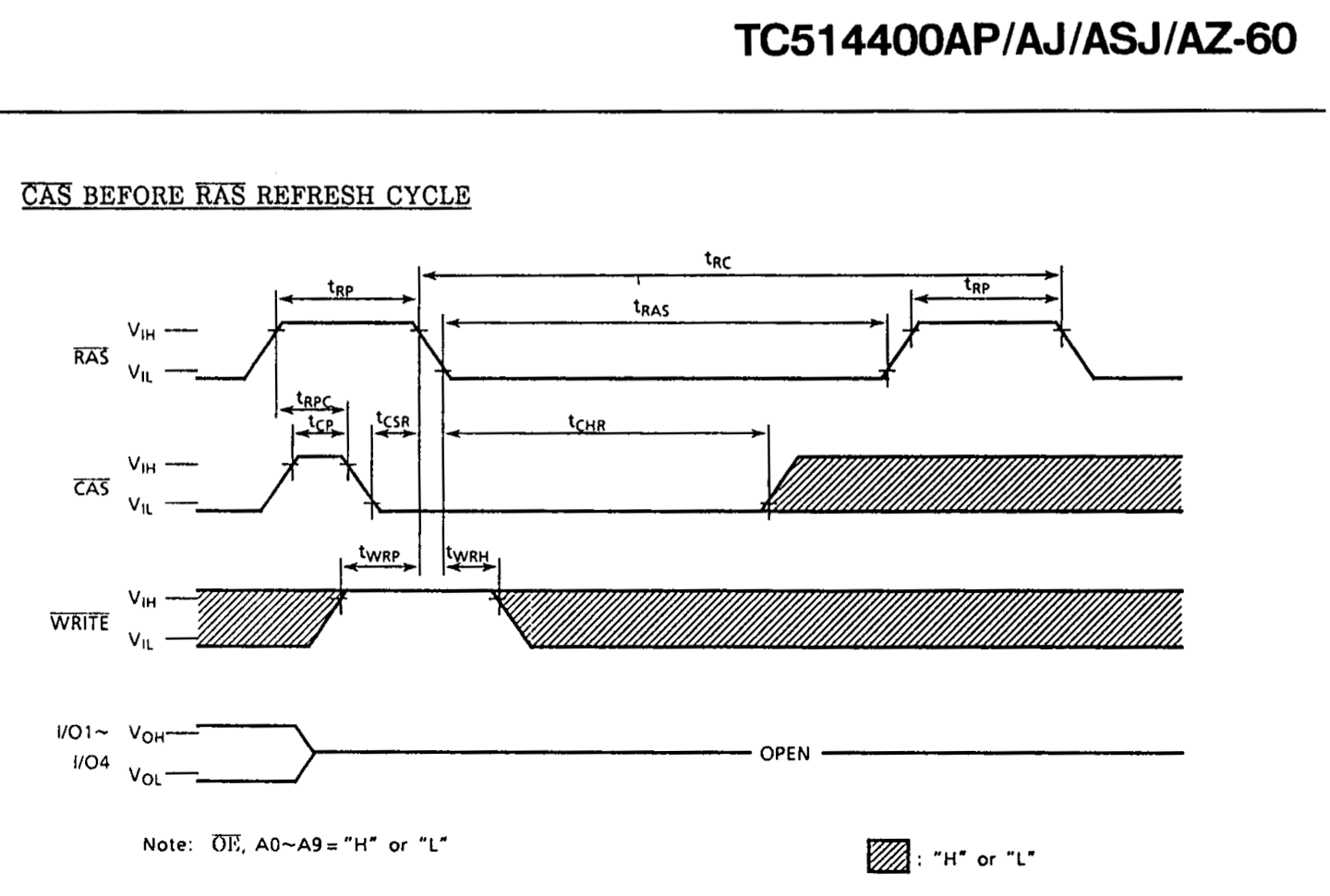
The IIgs follows the 1Mbit specification and the state of WE during a refresh cycle is undetermined (it is actually the state left by the transaction right before the refresh cycle). This behavior randomly enables the test mode in the memories with catastrophic results to the running programs.
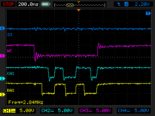
The the gates U3D, U3A and the flip-flop U2A form a refresh cycle detector. The Q output of the flip-flop is high if the system is performing a RAS before CAS refresh cycle. The flip-flop will latch the value of RAS at every falling edge for CAS (this will be high only during a RAS before CAS cycle). In any case the flip-flop will be cleared on the rising edge of CAS (all cycle types end with CAS de-assertion).
Based on the output of the flip-flop, U3C and U3B force WE high if a refresh cycle is in progress.
BOM Notes
U2 (dual D flip-flop) and U3 (quad NAND) propagation delay is critical for the proper operating of the card. Both should be F or ACT. U4 (quad 2-to-1 multiplexer) can be either fast (F or ACT) or slow (LS or HCT), however resistor values and location must be changed based on the chip speed. For best signal integrity U1 should be standard LS.
| Location | Fast | Slow |
|---|---|---|
| U4 | F or ACT | LS or HCT |
| R1 | 33 | DNI |
| R2 | 33 | DNI |
| R6 | DNI | 3.3 |
| R7 | DNI | 3.3 |