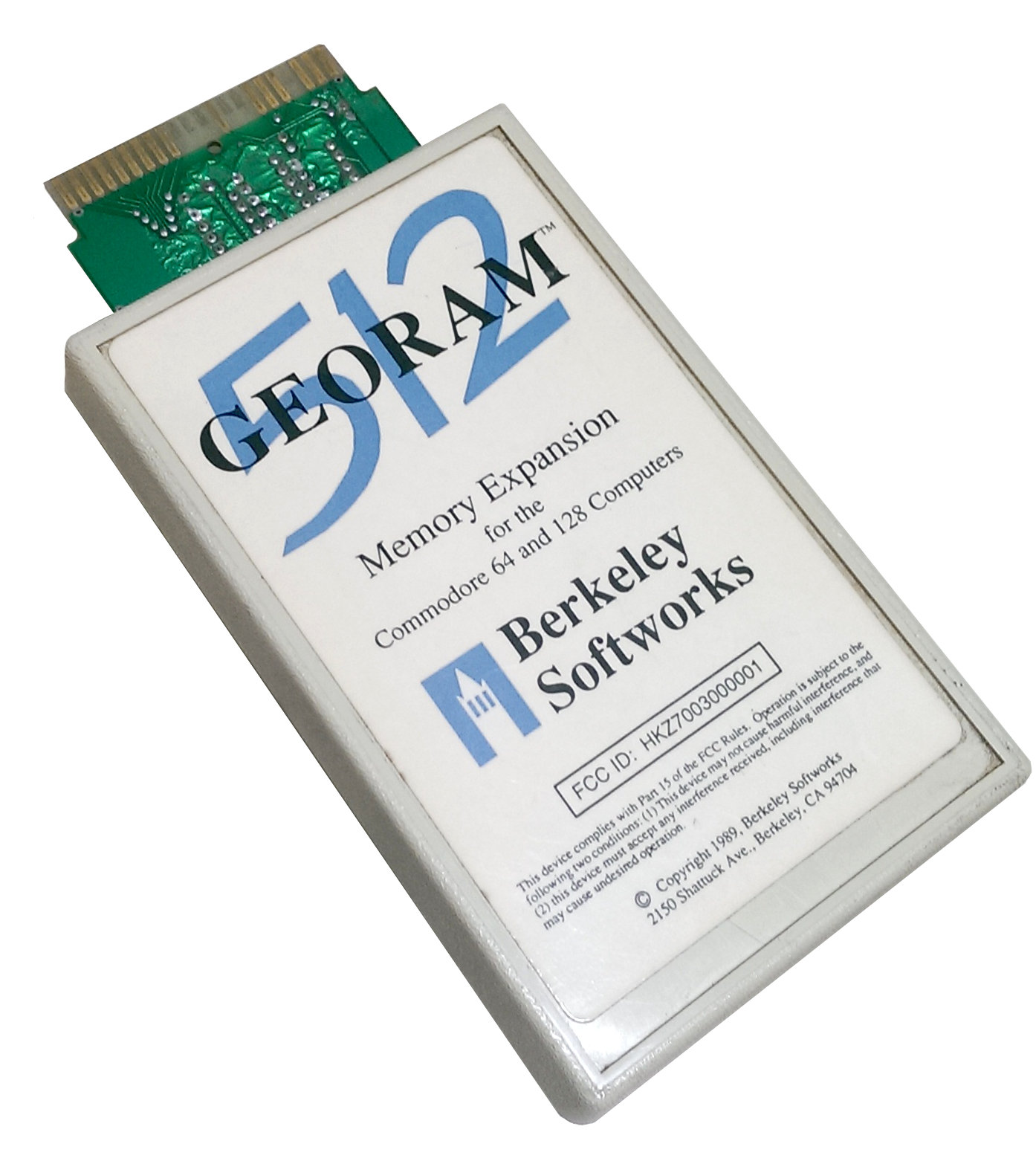
 This year our staff decided to enter the retrochallenge competition. Our goal is to reverse engineer the Berkely softworks geoRAM and publish what we discover under the GPL. The geoRAM is a 512KB memory expansion for the Commodore 64 and 128. Unlike the Commodore 1750 REU, which contain a custom chip, the geoRAM is built completely out of standard TTL chips.
The geoRAM is a banked system. The registers at $dfff and $dffe select which 256 bytes page is visible in the $de00-$deff range. The $dfff register selects a 16KB block out of the total memory, the register at $dffe selects the actual 256 bytes page within the selected block. Valid values for a standard geoRAM are 0-31 for the Block register and 0-63 for the page register. It is possible to extend the block register to 8-bit to create a 4MB geoRAM.
Teardown
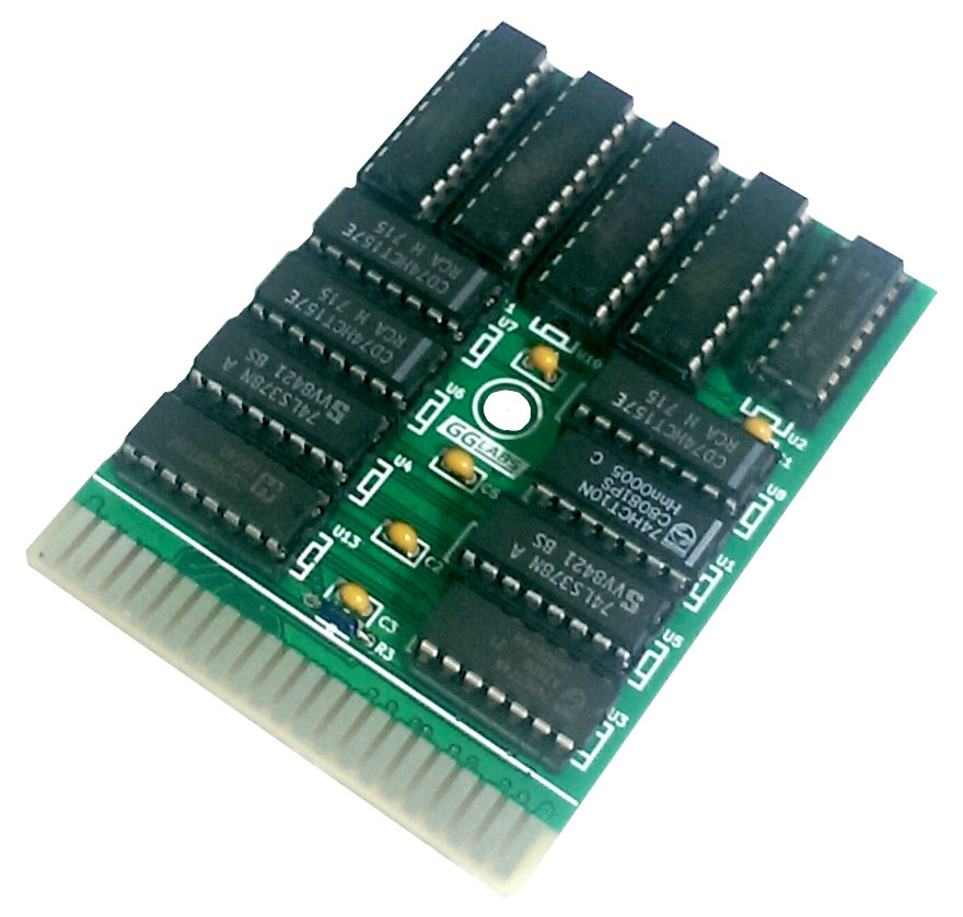
The picture below shows the full PCB without the plastic shell. It is easy to see the DRAM section with four 44C256 (256Kx4) memories. It is also easy to see the two 74HC378 6-bit registers that control the geoRAM paging scheme.
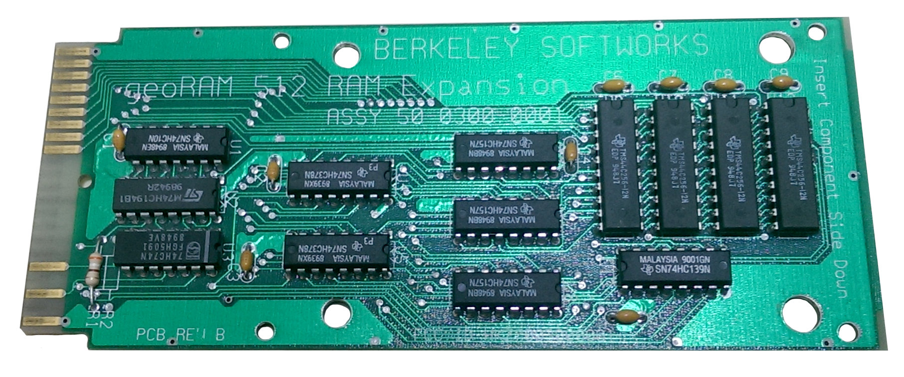
The full list of ICs used in the design is in the following table.
| Refdes | Part Numebr | Description | Notes |
|---|---|---|---|
| U1 | 74HC10 | Triple 3-input NAND Gate | State machine logic |
| U2 | 74HC194 | 4-bit Bidirectional Shift Register | State machine for DRAM access and refresh |
| U3 | 74HC74 | Dual D Flip−Flop with Set and Reset | State machine reset and register write enable |
| U4, U5 | 74HC378 | Hex D-Type Flip-Flop with Clock Enable | Paging registers |
| U6, U7, U8 | 74HC157 | Quad 2-input Multiplexer | Multiplex Rows and Columns |
| U9, U10, U11, U12 | 44C256 | 256 x 4 Bit CMOS Dynamic RAM with Fast Page Mode | 512KB total |
| U13 | 74HC139 | Dual 2-to-4 Line Decoder/Demultiplexer | Select for DRAM and registers |
Like most of the PCBs of the time the board is just 2-layers making reverse engineering quite easy. Simple visual inspection and an ohmmeter are sufficient to fully trace every single net in the design.
Schematics Description
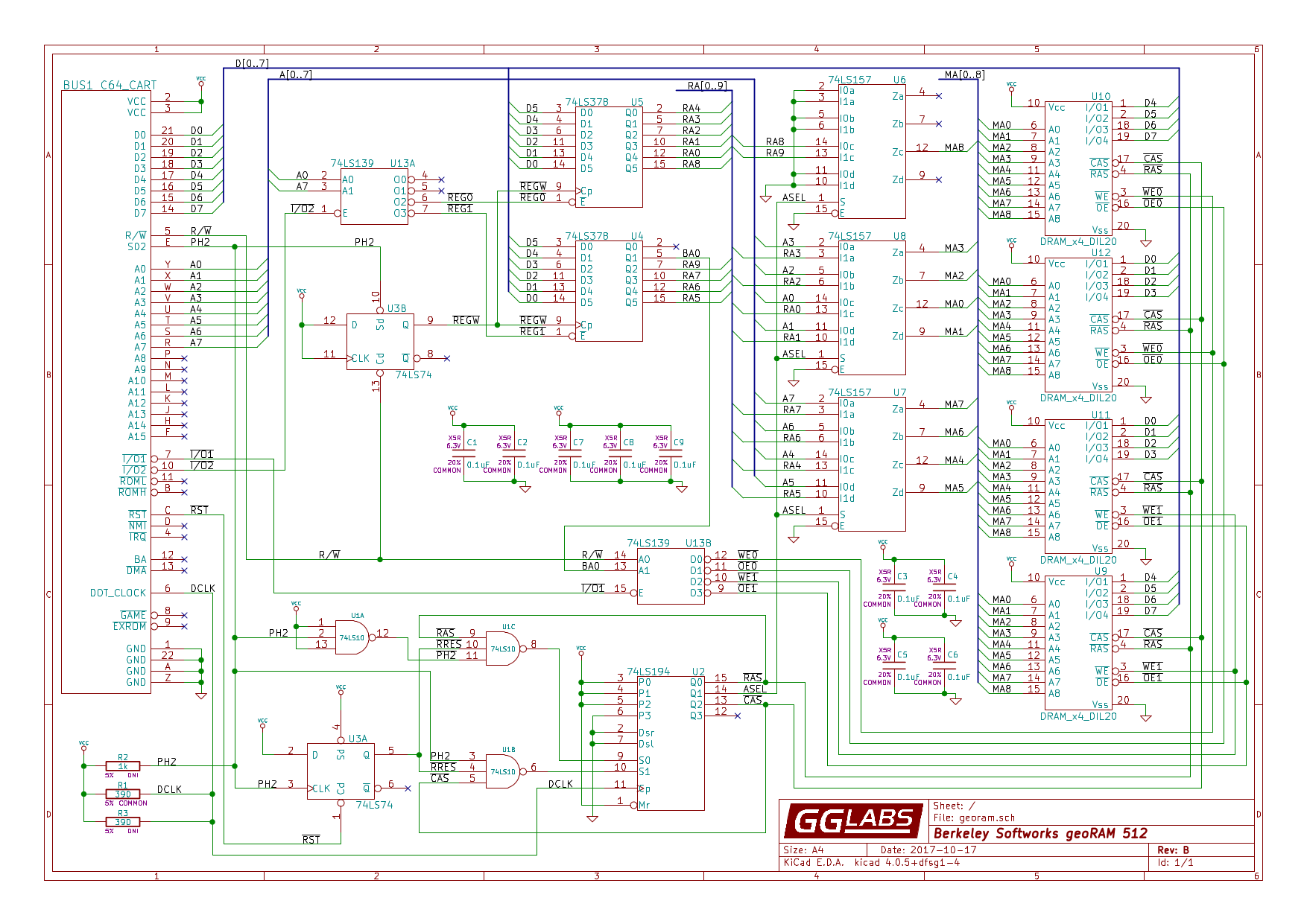
The schematics can be partitioned in a few main blocks. The register section is formed by U3B, U4, U5 and U13A. The decoder U13A select the correct register based on IO/2 (the system asserts this when the address is within $df00-$dfff), A0 and A7. Because of the incomplete decoding the two registers are mirrored in the range $df80-$dfff. U3B produces a clean clock for U4 and U5, if the enable is asserted a write to the register will occur. U4 maps to $dfff (block register) and U5 maps to $dffe (page register).
The memory section includes U6-8, U9-U12 and U13B. DRAMs require the address to be split into Row and Column which are multiplexed on the same pins. The three 74HC157 multiplexers (U6-U8) serve exactly this purpose. The U13B decoder selects the DRAM array if the I/O1 signal is asserted ($de00-$deff) and generates the output enable (OEx) or write enable (WEx) to the correct set of DRAMs. U10 and U12 map to the first 256KB of expanded memory while U9 and U11 map to the second 256KB section.
The memory control end refresh section includes U1, U2 and U3A. The circuit is very clever. A 4 bit bidirectional shift register is used to create a state machine that generates the RAS#, CAS# and SEL for both access cycles and refresh cycles. The state machine is clocked by the Commodore dot clock which is 8 times faster than PHI2. Memory refresh is performed while PHI2 is deasserted to allow the CPU to access the memory without any wait states.
| DOT_CLOCK | PHI2 | RAS# | SEL | CAS# | Notes |
|---|---|---|---|---|---|
| 0 | 1 | 1 | 1 | 1 | idle |
| 1 | 1 | 0 | 1 | 1 | RAS# asserted |
| 2 | 1 | 0 | 0 | 1 | SEL mux switch |
| 3 | 1 | 0 | 0 | 0 | CAS# asserted |
| 4 | 0 | 1 | 1 | 1 | idle |
| 5 | 0 | 1 | 1 | 0 | CAS# before RAS# refresh cycle |
| 6 | 0 | 1 | 0 | 0 | |
| 7 | 0 | 0 | 0 | 0 |
The table above shows the valid states and the sequences that are used. It's easy to notice that only 3 of the 4 bits are used and the shift register is reset at the beginning of every half PHI2 cycle with all ones. Then a single zero is shifted in for every dot_clock. The shift direction is determined by the level of the PHI2 clock giving the desired behavior of hidden refresh cycles. The U3A flip-flop is used to initialize the state machine to a known state upon exiting reset. U1A generates PHI2#. U1B and U1C generate the control signals for the shift register to implement the state machine. R1 sharpens the dot_clock rising edge to improve timing.
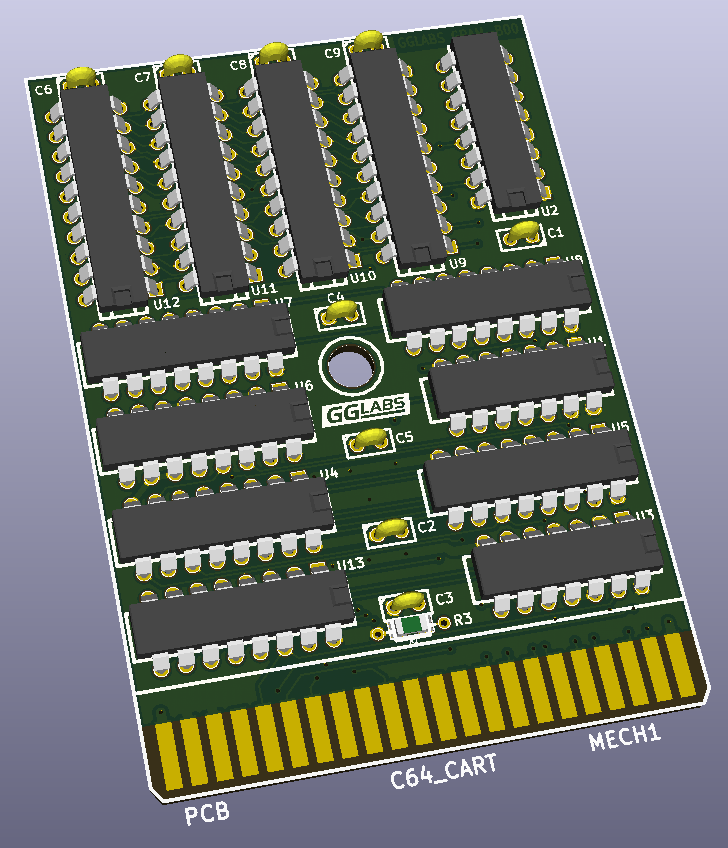
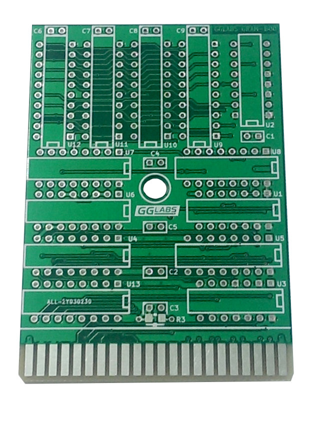
PCB Design
As this was mainly a documentation project, the schematics is a perfect replica of the original. No pin swaps or optimization have been performed, even the chip refdes have been preserved. The only difference from the original geoRAM is the final PCB form factor. Thanks to careful layout and modern tools it was possible to pack all the components inside a standard commodore cartridge.
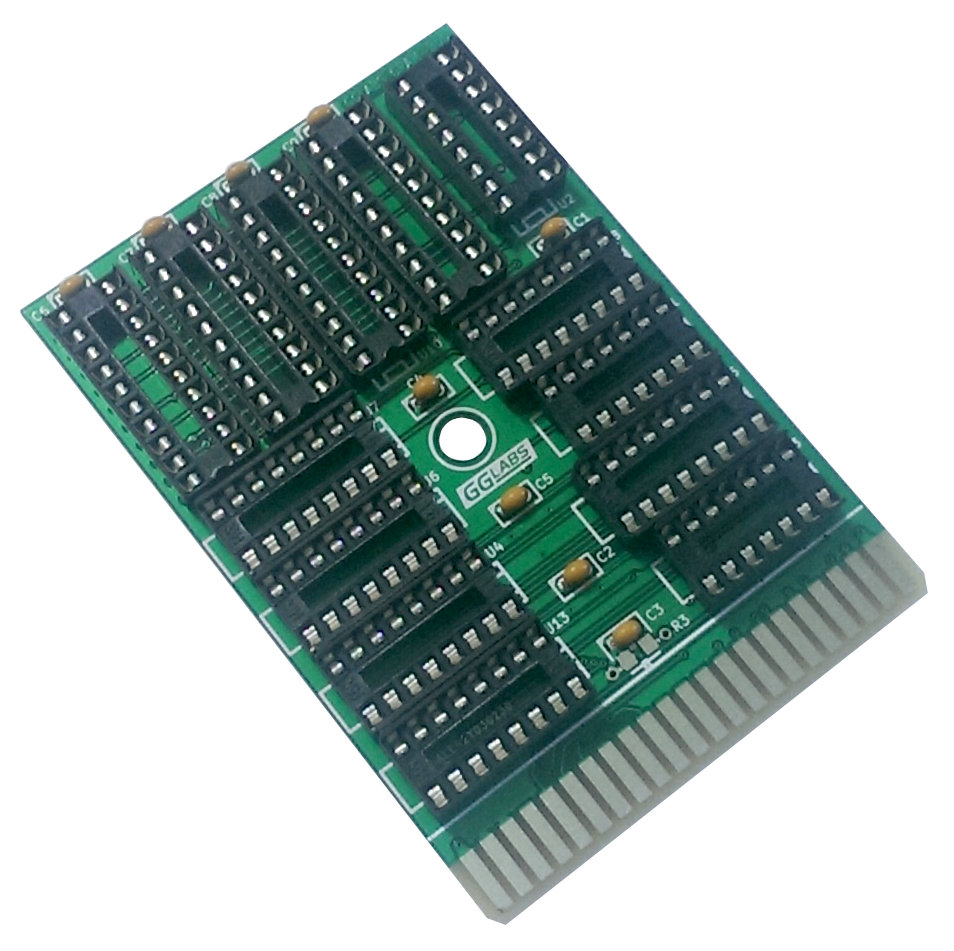
Board Assembly
The design is 100% through hole making manual assembly quite easy. The full BOM is in the table below. It is recommended to mount the resistor and the capacitors first. Then assemble all the sockets. The fit is quite tight, but there is just enough clearance to pack all of them in. Finally insert the chips in the sockets.
| Qty | Refdes | Part | Description |
|---|---|---|---|
| 1 | R1 | 390ohm 1/8w axial resistor | |
| 9 | C1,C2,C3,C4,C5,C6,C7,C8,C9 | 0.1uF X7R ceramic capacitors (3mm pitch) | |
| 1 | U1 | 74HC10 | Triple 3-input NAND Gate |
| 1 | U2 | 74HC194 | 4-bit Bidirectional Shift Register |
| 1 | U3 | 74HC74 | Dual D Flip−Flop with Set and Reset |
| 2 | U4, U5 | 74HC378 | Hex D-Type Flip-Flop with Clock Enable |
| 3 | U6, U7, U8 | 74HC157 | Quad 2-input Multiplexer |
| 4 | U9, U10, U11, U12 | KM44C256 | 256 x 4 Bit CMOS Dynamic RAM with Fast Page Mode |
| 1 | U13 | 74HC139 | Dual 2-to-4 Line Decoder/Demultiplexer |
DRAM Cross Reference
All 256Kx4 DRAM in DIP 20 can be used in the design. The table below shows a quick cross reference for convenience.
| Vendor | P/N |
|---|---|
| Samsung | KM44C256 |
| TI | TMS44C256 |
| Hyunday | HY534256 |
| Micron | MT4C4256 |
| NEC | uPD424256 |
| Toshiba | TC514256 |
| Hitachi | HM514256 |
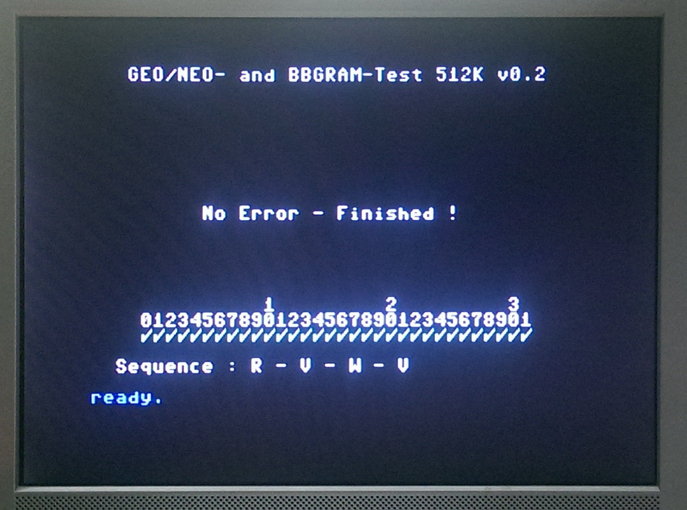
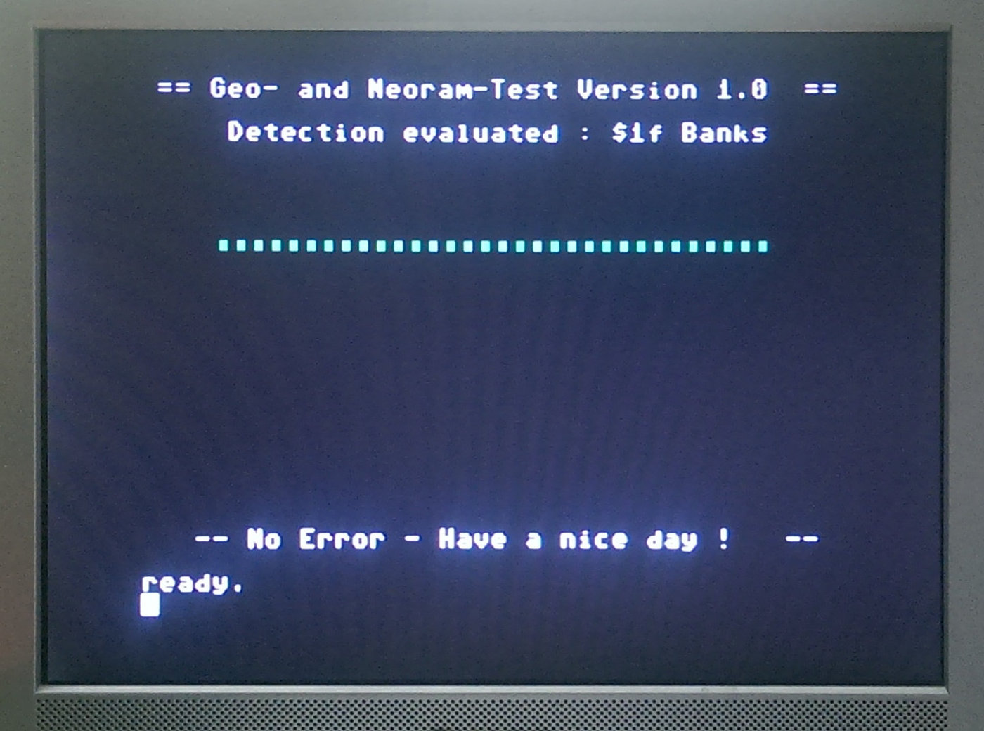
Testing
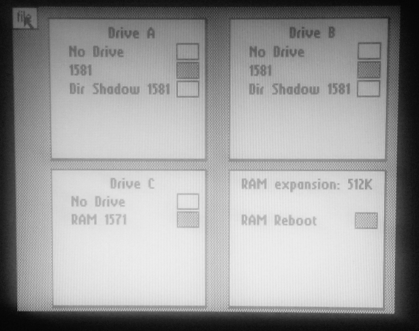
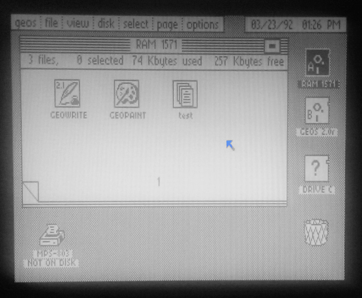
Testing has been performed using two different memory tests and running GEOS. It is important to note that GEOS 2.0r (which was originally shipped with the geoRAM) is required to take advantage of the memory expansion.
Previous versions of GEOS only support the Commodore REU.
We were not able to locate an original GEOS 2.0r image on the internet. Our solution was to download a D81 image of GEOS 2.0 and replace GEOBOOT and CONFIGURE with the correct geoRAM version.
All the required files can be downloaded from http://cbmfiles.com/geos/index.php